| CPC H01L 23/13 (2013.01) [H01L 23/49822 (2013.01); H01L 23/20 (2013.01); H01L 24/48 (2013.01); H01L 24/49 (2013.01); H01L 2224/48227 (2013.01); H01L 2224/49176 (2013.01); H01L 2924/15151 (2013.01); H01L 2924/15153 (2013.01); H01L 2924/17151 (2013.01)] | 20 Claims |
|
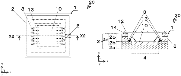
1. An electronic element mounting substrate comprising:
a substrate comprising, on a first upper surface, a mounting region in which an electronic element is to be mounted;
a frame body located on the first upper surface of the substrate and surrounding the mounting region;
a channel extending through the frame body outward from an inner wall of the frame body; and
an electrode pad located on the first upper surface of the substrate or an inner surface of the frame body, wherein
the channel is located above or below the electrode pad, and
the frame body comprises a first frame body located on the first upper surface of the substrate and surrounding the mounting region, and a second frame body located on and is in direct contact with a second upper surface of the first frame body and surrounding the mounting region.
|