| CPC H01L 22/20 (2013.01) [H01L 21/67248 (2013.01); H01L 21/67253 (2013.01)] | 17 Claims |
|
1. A substrate processing apparatus comprising:
a process chamber in which substrate processing is executed;
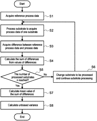
a memory that stores recipe information describing a procedure that executes the substrate processing, process data measured during executing processing of a substrate in the process chamber, data calculated from the process data, and comparison data to be compared with the data; and
a calculator configured to be capable of comparing the data with the comparison data to obtain an index indicating a reproducibility of the comparison data, and calculating a value of setting information included in the recipe information when the index is smaller than a predetermined value.
|