| CPC H01L 22/12 (2013.01) [H01J 37/28 (2013.01); H01L 21/76802 (2013.01); H01L 21/76834 (2013.01); H01L 21/76877 (2013.01); H01L 23/5283 (2013.01); H10B 63/84 (2023.02); G11C 13/0004 (2013.01); G11C 13/0026 (2013.01); G11C 13/0028 (2013.01); G11C 13/004 (2013.01); G11C 13/0069 (2013.01); G11C 2213/71 (2013.01); H01J 37/04 (2013.01); H01J 2237/2804 (2013.01); H01J 2237/2814 (2013.01); H10N 70/231 (2023.02); H10N 70/826 (2023.02); H10N 70/8825 (2023.02)] | 18 Claims |
|
1. An apparatus, comprising:
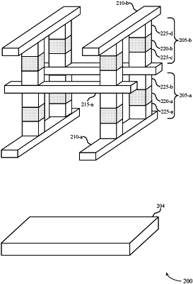
a substrate coupled with a test stage, the substrate at a first level of a memory device;
a set of access lines for the memory device, the set of access lines at a second level of the memory device and comprising a first material;
a first set of lines comprising the first material and at the second level of the memory device, the first set of lines each electrically floating; and
a second set of lines comprising the first material and at the second level of the memory device, the second set of lines each coupled with a ground reference.
|