| CPC H01L 21/67196 (2013.01) [H01L 21/67167 (2013.01); H01L 21/68707 (2013.01); H01L 21/67207 (2013.01)] | 15 Claims |
|
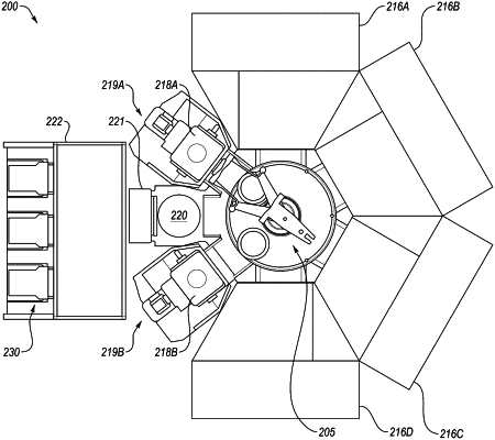
1. A substrate processing system comprising:
a factory interface having a controlled environment;
a transfer chamber of heptagonal shape and comprising:
four first facets; and
three second facets, wherein each of the three second facets has a width that is narrower than that of each of the four first facets;
a first processing chamber attached to one of the four first facets;
a first auxiliary chamber attached to a first of the three second facets, wherein the first auxiliary chamber is smaller than the first processing chamber;
a load lock attached to a second of the three second facets and to the factory interface; and
a robot attached to a bottom of the transfer chamber, the robot adapted to transfer substrates to and from the first processing chamber, the first auxiliary chamber, and the load lock, wherein a distance between a center of the robot and a center of one of the first auxiliary chamber is within 20% of 35 inches.
|