| CPC H01G 4/30 (2013.01) [H01G 4/012 (2013.01); H01G 4/1227 (2013.01); H01G 13/06 (2013.01)] | 23 Claims |
|
1. A multilayer electronic component comprising:
a body including a plurality of dielectric layers and a plurality of internal electrodes alternately disposed with the dielectric layers in a first direction, and having first and second surfaces opposing each other in the first direction, third and fourth surfaces connected to the first and second surfaces and opposing each other in a second direction, and fifth and sixth surfaces connected to the first to fourth surfaces and opposing each other in a third direction; and
external electrodes disposed on the body,
wherein:
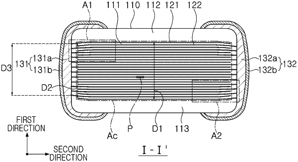
when a region in which the plurality of internal electrodes overlap each other in the first direction is defined as a capacitance forming portion, the plurality of internal electrodes include internal electrodes that are curved at end portions thereof in the capacitance forming portion and internal electrodes that are flat in the capacitance forming portion,
in a cross-section of the body in the first and second directions, (F1+F2)/D1×100 is 35 or less, where F1 is a maximum distance from an uppermost internal electrode to an uppermost flat internal electrode in the first direction, F2 is a maximum distance from a lowermost internal electrode to a lowermost flat internal electrode in the first direction, and D1 is a size of the capacitance forming portion in the first direction at a center thereof in the second direction, and
the external electrodes include first and second external electrodes disposed on the third and fourth surfaces, respectively, and the plurality of internal electrodes includes the first internal electrodes connected to the first external electrode at the third surface, and second internal electrodes connected to the second external electrode at the fourth surface.
|