| CPC G11C 8/10 (2013.01) [G11C 8/08 (2013.01); G11C 8/18 (2013.01)] | 11 Claims |
|
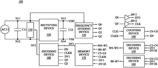
1. A memory chip, comprising:
a first encoding device configured to generate a plurality of word line signals; and
a memory device configured to generate a third data signal according to a first data signal and a second data signal, the memory device comprises:
a first memory circuit configured to generate the first data signal according to the plurality of word line signals at a first node during a first period; and
a second memory circuit configured to generate the second data signal according to the plurality of word line signals at a second node different from the first node during a second period after the first period.
|