| CPC G11C 16/0483 (2013.01) [G11C 8/14 (2013.01); H01L 23/481 (2013.01); H10B 41/10 (2023.02); H10B 41/27 (2023.02); H10B 41/35 (2023.02); H10B 43/10 (2023.02); H10B 43/27 (2023.02); H10B 43/35 (2023.02)] | 19 Claims |
|
1. A semiconductor structure comprising a memory die, wherein the memory die comprises:
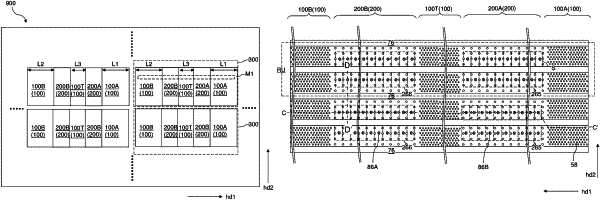
an alternating stack of insulating layers and electrically conductive layers overlying a substrate and laterally extending through a series of regions that comprises, in a spatial order along a first horizontal direction, a first contact region, a first memory array region, a second contact region, a second memory array region, a third contact region, and a third memory array region;
arrays of memory openings located in the first memory array region, the second memory array region, and the third memory array region; and
arrays of memory opening fill structures located within the arrays of memory openings, wherein each of the memory opening fill structures comprises a respective vertical stack of memory elements.
|