| CPC G11C 11/5642 (2013.01) [G11C 5/14 (2013.01); G11C 11/5671 (2013.01); G11C 16/0483 (2013.01); G11C 16/26 (2013.01); G11C 16/30 (2013.01)] | 11 Claims |
|
1. A semiconductor memory device comprising:
a substrate having a surface extending in a first direction and in a second direction crossing the first direction;
a first memory cell provided on one side of the substrate in a third direction crossing the first direction and the second direction;
a first select transistor electrically connected to the first memory cell and provided on one side of the first memory cell in the third direction;
a second memory cell provided on the one side of the substrate in the third direction;
a second select transistor electrically connected to the second memory cell and provided on one side of the second memory cell in the third direction;
a first word line extending in the first direction and connected to a gate of the first memory cell and a gate of the second memory cell;
a first select gate line extending in the first direction and connected to a gate of the first select transistor;
a second select gate line extending in the first direction and connected to a gate of the second select transistor;
a first bit line electrically connected to the first select gate transistor and the second select gate transistor;
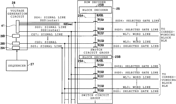
a voltage generation circuit configured to independently drive the first select gate line and the second select gate line; and
a sequencer configured to perform a first read operation to read data from the first memory cell and a second read operation to read data from the second memory cell, wherein
in the first read operation, the voltage generation circuit applies a first voltage to the first word line, applies a second voltage to the first select gate line, and applies a third voltage to the second select gate line, and
in the second read operation, the voltage generation circuit applies a fourth voltage to the first word line, applies a fifth voltage to the first select gate line, and applies a sixth voltage, which is different from the second voltage, to the second select gate line.
|