| CPC G11C 11/5628 (2013.01) [G11C 11/5671 (2013.01); G11C 16/0483 (2013.01); G11C 16/10 (2013.01); G11C 16/3459 (2013.01); H01L 25/0657 (2013.01); H01L 2225/06506 (2013.01); H01L 2225/06562 (2013.01); H10B 41/27 (2023.02); H10B 43/27 (2023.02)] | 15 Claims |

|
1. A method of performing a write in a semiconductor storage device, said method comprising:
programming a memory transistor of the semiconductor storage device;
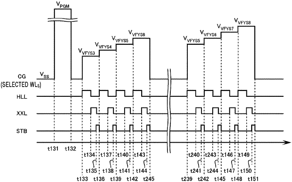
executing a plurality of verification operations in sequence after programming the memory transistor, the verification operations including a first verification operation, a second verification operation that completes execution after the first verification operation, a third verification operation that completes execution after the second verification operation, and a fourth verification operation that completes execution after the third verification operation, wherein during the first, second, third, and fourth verification operations, voltages of first, second, third, and fourth levels are applied to a word line that is electrically connected to the memory transistor, respectively; and
upon receipt of a command to resume a write sequence that was interrupted before the fourth verification operation completed, prior to re-executing the fourth verification operation, executing at least one but no more than two verifications operations.
|