| CPC G11C 11/4091 (2013.01) | 19 Claims |
|
1. A memory device, comprising:
a capacitor;
a first transistor having a first end coupled to the capacitor;
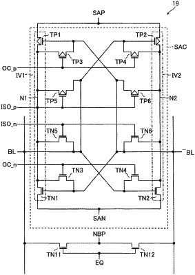
a first inverter circuit which is coupled between a first node and a second node, and which includes a p-type second transistor and an n-type third transistor that are coupled in series at a third node;
a second inverter circuit which is coupled between the first node and the second node, and which includes a p-type fourth transistor and an n-type fifth transistor that are coupled in series at a fourth node, a gate of the fourth transistor and a gate of the fifth transistor being coupled to a second end of the first transistor;
a sixth transistor coupled between the gate of the fourth transistor and the third node and between the gate of the fifth transistor and the third node;
a seventh transistor coupled between a gate of the second transistor and the fourth node and between a gate of the third transistor and the fourth node;
an eighth transistor coupled between the gate of the second transistor and the third node; and
a ninth transistor coupled between the gate of the fourth transistor and the fourth node.
|