| CPC G11C 11/405 (2013.01) [H01L 27/1207 (2013.01); H01L 27/1225 (2013.01); H01L 27/1255 (2013.01); H01L 29/78648 (2013.01); H01L 29/7869 (2013.01); H10B 12/00 (2023.02)] | 9 Claims |
|
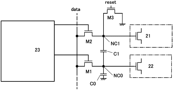
1. A memory circuit comprising:
a first transistor and a second transistor which are electrically connected to a data line;
a memory controller electrically connected to a gate of the first transistor and a gate of the second transistor;
a third transistor whose off state is switched to an on state by a reset signal applied to a gate of the third transistor, wherein a first node is reset in the on state; and
a first capacitor and a second capacitor connected in series,
wherein one of a source and a drain of the second transistor is electrically connected to the data line,
wherein one of a source and a drain of the third transistor is electrically connected to one electrode of the first capacitor, and the other electrode of the first capacitor is electrically connected to one of a source and a drain of the first transistor,
wherein the one electrode of the first capacitor is electrically connected to the one of the source and the drain of the second transistor,
wherein the other electrode of the first capacitor is electrically connected to one electrode of the second capacitor, and a second node is formed between the first capacitor and the second capacitor, and
wherein the first node and the second node are configured to retain different potentials.
|