| CPC G11C 11/405 (2013.01) [G11C 11/4096 (2013.01); H01L 27/1207 (2013.01); H01L 27/1225 (2013.01); H01L 27/124 (2013.01); H01L 27/1255 (2013.01); H01L 29/78648 (2013.01); H01L 29/7869 (2013.01); H10B 12/00 (2023.02)] | 8 Claims |
|
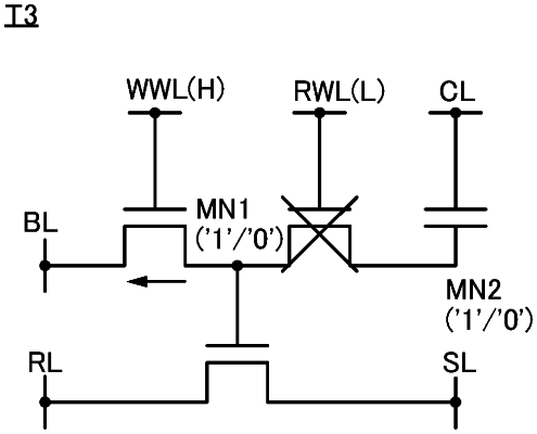
1. A semiconductor device comprising:
a first transistor;
a second transistor; and
a third transistor,
wherein one of a source and a drain of the first transistor is electrically connected to a first wiring for reading data,
wherein one of a source and a drain of the second transistor is electrically connected to a first node and a gate of the first transistor,
wherein the other of the source and the drain of the second transistor is electrically connected to a second wiring for writing the data,
wherein one of a source and a drain of the third transistor is electrically connected to the first node and the gate of the first transistor,
wherein the other of the source and the drain of the third transistor is electrically connected to a second node and a capacitor for retaining electric charge corresponding to the data,
wherein the third transistor comprises a metal oxide in a channel formation region, and
wherein during data retention operation, a potential of the first node is changed to be different from a potential of the second node by turning off the third transistor while the second transistor is in a conduction state.
|