| CPC G11C 11/1675 (2013.01) [G11C 11/1655 (2013.01); G11C 11/1657 (2013.01); G11C 11/1673 (2013.01)] | 16 Claims |
|
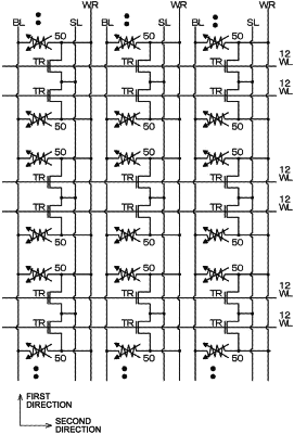
1. A nonvolatile memory cell comprising:
a resistance-change nonvolatile memory element and a selection transistor, wherein
one end of the nonvolatile memory element is connected to one source/drain region of the selection transistor and is connected to a write line,
other source/drain region of the selection transistor is connected to a select line,
another end of the nonvolatile memory element is connected to a bit line,
the selection transistor and the write line are provided on a first surface side of a base portion made of a semiconductor material, and
the nonvolatile memory element is provided on a second surface side opposing the first surface of the base portion.
|