| CPC G09G 5/008 (2013.01) [G09G 2370/04 (2013.01)] | 20 Claims |
|
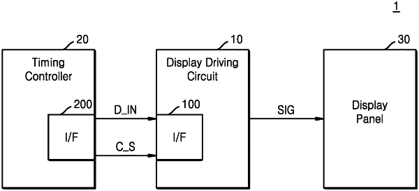
1. A display driving circuit comprising:
a clock data recovery circuit configured to:
receive a data signal, and
generate a clock signal and a first output data signal, the clock data recovery circuit comprising a jitter generator configured to generate jitter of the clock signal and vary an amplitude the jitter according to a horizontal control signal;
an eye margin test circuit configured to:
sample the data signal by using the clock signal, based on a vertical measurement voltage, and
generate a second output data signal based on the sampled data signal; and
a bit error check circuit configured to measure a bit error rate of the data signal, based on the first output data signal and the second output data signal.
|