| CPC G09G 3/3677 (2013.01) [G09G 2300/0876 (2013.01)] | 20 Claims |

|
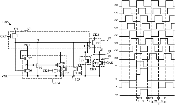
1. A gate driving circuit, comprising a plurality of cascaded gate driving units, each of the driving units comprising:
a pull-up control module, electrically connected to a first node, configured to control a voltage level of the first node;
a pull-up module, electrically connected to the first node and a scan signal output end of a current stage, configured to pull up a voltage level of the scan signal output end of the gate driving unit of a current stage under a control of the voltage level of the first node;
a pull-down module, electrically connected to the scan signal output end of the gate driving unit of the gate driving unit of the current stage, configured to pull down the voltage level of the scan signal output end of the gate driving unit of the current stage; and
a pull-down control module, electrically connected to a second node, the first node, a first clock signal end and the scan signal output end of the gate driving unit of the current stage, configured to periodically pull down a voltage level of the second node under a control of an input signal of the first clock signal end to maintain the voltage level of the first node and the voltage level of the scan signal output end of the gate driving unit of the current stage.
|