| CPC G09G 3/3275 (2013.01) [H10K 59/121 (2023.02); G09G 2310/0297 (2013.01)] | 6 Claims |
|
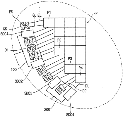
1. A display device comprising:
a substrate including a circular display area and a non-display area surrounding the display area;
a plurality of pixels including a first pixel, a second pixel, a third pixel, and a fourth pixel disposed on the display area of the substrate;
a first sub-demux circuit connected to the first pixel and disposed on the non-display area to transfer a first data output signal to the first pixel;
a second sub-demux circuit connected to the second pixel and disposed on the non-display area to transfer a second data output signal to the second pixel;
a third sub-demux circuit connected to the third pixel and disposed on the non-display area to transfer a third data output signal to the third pixel;
a fourth sub-demux circuit connected to the fourth pixel and disposed on the non-display area to transfer a fourth data output signal to the fourth pixel;
a first connection line connected to the first sub-demux circuit and the second sub-demux circuit and disposed on the non-display area to transfer a first data input signal to the first sub-demux circuit and transfer a second data input signal to the second sub-demux circuit;
a second connection line connected to the third sub-demux circuit and the fourth sub-demux circuit and dispose on the non-display area to transfer a third data input signal to the third sub-demux circuit and transfer a fourth data input signal to the fourth sub-demux circuit,
wherein a distance between the first sub-demux circuit and the second sub-demux circuit connected to the first connection line is different from a distance between the third sub-demux circuit and the fourth sub-demux circuit connected to the second connection line; and
a plurality of gate stages connected to the pixels and disposed on the non-display area to transfer gate signals to the pixels,
wherein some of the gate stages are disposed between the first sub-demux circuit and the second sub-demux circuit, and
wherein another of the gate stages are disposed between the second sub-demux circuit and the third sub-demux circuit, and
wherein still another of the gate stages are disposed between the third sub-demux circuit and the fourth sub-demux circuit,
wherein a number of light emitting stages disposed between the first sub-demux circuit and the second sub-demux circuit is different from a number of light emitting stages disposed between the third sub-demux circuit and the fourth sub-demux circuit.
|