| CPC G09G 3/3266 (2013.01) [G09G 2320/0247 (2013.01)] | 25 Claims |
|
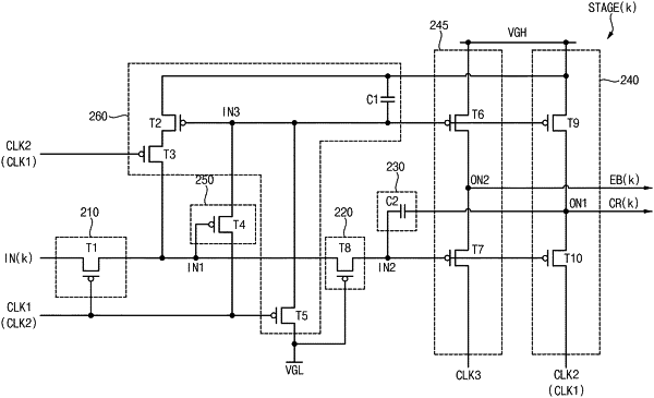
1. A scan driver for applying a bias voltage, the scan driver comprising:
first to nth stages, where n is an integer of 2 or more, configured to output first to nth output signals for applying the bias voltage to first to nth pixel rows, respectively,
wherein the kth stage, where k is an integer of 1 to n, includes:
an inputter configured to transmit an input signal to a first node in response to a first clock signal;
a stress reliever disposed between the first node and a second node;
a carry signal outputter configured to receive a high power supply voltage and a second clock signal and to output the second clock signal as a kth carry signal through a first output node in response to a voltage of the second node;
an output signal outputter configured to receive the high power supply voltage and a third clock signal and to output the third clock signal as the kth output signal through a second output node in response to the voltage of the second node;
a maintainer configured to transmit the first clock signal to a third node in response to a voltage of the first node; and
a stabilizer configured to apply a first low power supply voltage to the third node in response to the first clock signal and to apply the high power supply voltage to the first node in response to the second clock signal, and
wherein each of the first clock signal and the second clock signal selectively toggles between the high power supply voltage and the first low power supply voltage, the third clock signal selectively toggles between the high power supply voltage and a second low power supply voltage different from the first low power supply voltage, and the bias voltage is adjusted by changing the second low power supply voltage.
|