| CPC G09G 3/3258 (2013.01) [G09G 3/3233 (2013.01); G09G 2300/0819 (2013.01); G09G 2300/0852 (2013.01); G09G 2310/08 (2013.01); G09G 2320/0247 (2013.01); G09G 2340/0435 (2013.01)] | 6 Claims |
|
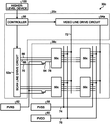
1. A display device comprising:
a light-emitting element,
a drive transistor coupled to the light-emitting element, a gate of the drive transistor is configured to receive an initialization voltage and a video voltage, and
a shut-off circuit, coupled to the drive transistor, configured to supply or shut off a power voltage to the drive transistor,
wherein,
the shut-off circuit is configured to supply the power voltage to the drive transistor while the initialization voltage is written into the gate of the drive transistor, and then shut off the power voltage while the video voltage is written into the drive transistor, and then supply the power voltage in an emission-enabled period at a black insertion rate which is a ratio of a period in which the power voltage is shut off to a period of the emission-enabled period,
a luminance set value corresponds to the black insertion rate and a voltage difference between the initialization voltage and the video voltage,
as the luminance set value gets lower, the black insertion rate and the initialization voltage get higher,
a gate-source voltage corresponds to the luminance set value, and
the black insertion rate is based on the initialization voltage and the luminance set value, such that a difference in black insertion rate increases relative to a difference in the initialization voltage, as the luminance set value gets lower, and as the initialization voltage gets higher.
|