| CPC G09G 3/20 (2013.01) [G09G 3/3266 (2013.01); G09G 3/3677 (2013.01); G09G 2300/0819 (2013.01); G09G 2300/0842 (2013.01); G09G 2310/0286 (2013.01); G09G 2310/04 (2013.01); G09G 2330/021 (2013.01); G09G 2340/0435 (2013.01)] | 20 Claims |
|
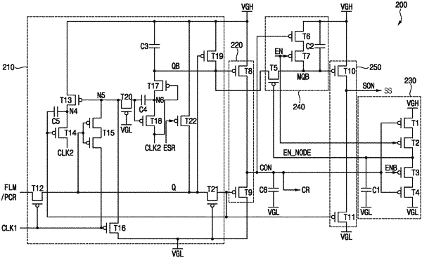
1. A scan driver including a plurality of stages, each of the plurality of stages comprising:
a control circuit which controls a voltage of a first node and a voltage of a second node in response to an input signal, a first clock signal and a second clock signal;
a carry output circuit which outputs a carry signal in response to the voltage of the first node and the voltage of the second node;
an enable node controlling circuit which controls a voltage of an enable node in response to the carry signal, an enable signal and an inverted enable signal;
a masking circuit which controls a voltage of a third node in response to the voltage of the second node and the voltage of the enable node; and
a scan output circuit which outputs a scan signal in response to the voltage of the first node and the voltage of the third node.
|