| CPC G06F 3/0445 (2019.05) [G06F 3/0412 (2013.01); G06F 3/0446 (2019.05)] | 30 Claims |
|
1. A touch display device comprising:
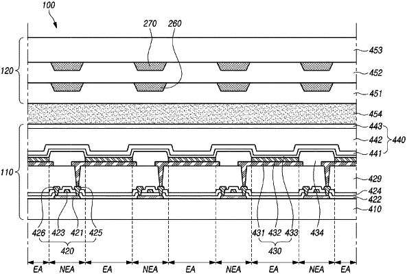
a display panel comprising an active area and a non-active area surrounding the active area; and
a touch panel disposed on the display panel, the touch panel including:
a first insulating layer disposed on the display panel;
a second insulating layer disposed on the first insulating layer;
a third insulating layer disposed on the second insulating layer;
a fourth insulating layer disposed between the display panel and the first insulating layer, the fourth insulating layer having an adhesive property;
a plurality of first touch electrodes disposed between the first insulating layer and the second insulating layer;
a plurality of second touch electrodes disposed between the second insulating layer and the third insulating layer;
a first touch pad electrode disposed in a touch pad area overlapped with the non-active area, the first touch pad electrode and the plurality of first touch electrodes being disposed in a same layer as each other; and
a second touch pad electrode in direct contact with the first touch pad electrode, the second touch pad electrode and the plurality of second touch electrodes being disposed in a same layer as each other, the second touch pad electrode being between the second insulating layer and the third insulating layer;
wherein each of the plurality of first touch electrodes overlaps a respective one of the plurality of second touch electrodes,
wherein a refractive index of each of the first insulating layer, the second insulating layer and the third insulating layer is the same,
wherein an upper surface of the first insulating layer is in contact with the plurality of first touch electrodes and a rear surface thereof has a flat shape, and an upper surface of the second insulating layer is in contact with the plurality of second touch electrodes and a rear surface thereof has a flat shape, and
wherein the upper surface of the first insulating layer is in contact with the rear surface of the second insulating layer and the rear surface of the first insulating layer is in contact with the fourth insulating layer.
|