| CPC G06F 3/0443 (2019.05) [G06F 3/0412 (2013.01); G06F 3/0446 (2019.05); H01L 24/04 (2013.01); H01L 24/16 (2013.01); H01L 24/29 (2013.01); H01L 24/32 (2013.01); H01L 24/73 (2013.01); H10K 50/844 (2023.02); H10K 59/131 (2023.02); H10K 59/40 (2023.02); H10K 59/88 (2023.02); H10K 77/111 (2023.02); G06F 2203/04111 (2013.01); H01L 2224/02145 (2013.01); H01L 2224/0221 (2013.01); H01L 2224/04026 (2013.01); H01L 2224/16148 (2013.01); H01L 2224/29198 (2013.01); H01L 2224/32148 (2013.01); H01L 2224/73204 (2013.01); H01L 2924/1426 (2013.01)] | 20 Claims |
|
1. A display apparatus, comprising:
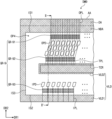
a substrate comprising a display region and a non-display region adjacent to the display region;
pixels disposed in the display region and connected to data lines;
output pad lines connected to the pixels;
output pads connected to the input pad lines;
a driving circuit chip disposed in the non-display region;
an encapsulation layer covering the pixels; and
a touch sensor disposed on the encapsulation layer and the touch sensor comprising a touch insulating layer comprising a first intaglio pattern defined by penetrating the touch insulating layer, and touch electrode layer, and
wherein the output pad lines are connected to the output pads across the first intaglio pattern.
|
|
11. A display apparatus, comprising:
a substrate comprising a display region and a non-display region adjacent to the display region;
pixels disposed in the display region and connected to data lines;
a pad group comprising input pad lines and input pads connected to the input pad lines;
a driving circuit chip disposed in the non-display region;
a flexible printed circuit board disposed in non-display region;
an encapsulation layer covering the pixels; and
a touch sensor disposed on the encapsulation layer and the touch sensor comprising a touch insulating layer comprising a first intaglio pattern defined by penetrating the touch insulating layer, and touch electrode layer, and
wherein the input pad lines connect the input pads and the flexible printed circuit board.
|