| CPC G06F 3/0412 (2013.01) [G06F 3/04164 (2019.05); G06F 3/044 (2013.01); G06F 3/0443 (2019.05); G06F 3/0446 (2019.05); G02F 1/3501 (2013.01); G06F 2203/04102 (2013.01); G06F 2203/04112 (2013.01)] | 9 Claims |
|
1. A display device comprising:
a base layer;
a buffer layer disposed on the base layer;
a display element layer disposed on the buffer layer and comprising a plurality of pixels, each of the pixels comprising an anode electrode, a cathode electrode, and a light emitting layer between the anode electrode and the cathode electrode;
an encapsulation layer disposed on the display element layer and covering the pixels;
a plurality of touch sensors disposed directly on the encapsulation layer, each of the touch sensors comprising a plurality of conductive patterns having a mesh shape; and
a plurality of signal lines respectively connected to the touch sensors,
wherein:
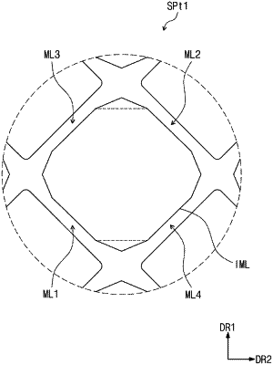
the conductive patterns comprise a plurality of mesh lines defining a plurality of mesh openings;
each of interior angles of one of the mesh openings is greater than 90 degrees;
the base layer comprises a bending area configured to bend about a bending axis;
the one of the mesh openings comprises at least five of the inner lines, and
at least one of the inner lines defining the one of the mesh openings is inclined with respect to the bending axis.
|