| CPC G06F 12/1466 (2013.01) [G06F 11/0772 (2013.01); G06F 11/1068 (2013.01); G06F 12/0853 (2013.01); G06F 12/1408 (2013.01)] | 21 Claims |

|
1. An apparatus, comprising processing circuitry to:
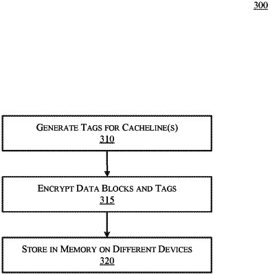
generate, for a cacheline, a first tag and a second tag, the first tag and the second tag generated as a function of user data stored and metadata in the cacheline stored in a first memory device, and a multiplication parameter derived from a secret key;
store the user data, the metadata, the first tag and the second tag in the cacheline of the first memory device;
generate, for the cacheline, a third tag and a fourth tag, the third tag and the fourth tag generated as a function of the user data stored and metadata in the cacheline stored in a second memory device, and the multiplication parameter;
store the user data, the metadata, the third tag and the fourth tag in a corresponding cacheline of the second memory device;
receive, from a requesting device, a read operation directed to the cacheline; and
use the first tag, the second tag, the third tag, and the fourth tag to determine whether a read error occurred during the read operation.
|