US 11,994,930 B2
Optimizing power in a memory device
Dinesh Patil, Sunnyvale, CA (US); Amir Amirkhany, Sunnyvale, CA (US); Farrukh Aquil, San Diego, CA (US); Kambiz Kaviani, Palo Alto, CA (US); and Frederick A. Ware, Los Altos Hills, CA (US)
Assigned to Rambus Inc., San Jose, CA (US)
Filed by Rambus Inc., San Jose, CA (US)
Filed on May 19, 2022, as Appl. No. 17/748,704.
Application 17/748,704 is a continuation of application No. 16/947,973, filed on Aug. 26, 2020, granted, now 11,340,686.
Application 16/947,973 is a continuation of application No. 16/193,247, filed on Nov. 16, 2018, granted, now 10,761,587, issued on Sep. 1, 2020.
Application 16/193,247 is a continuation of application No. 15/589,651, filed on May 8, 2017, granted, now 10,133,338, issued on Nov. 20, 2018.
Application 15/589,651 is a continuation of application No. 15/248,364, filed on Aug. 26, 2016, granted, now 9,645,631, issued on May 9, 2017.
Application 15/248,364 is a continuation of application No. 14/405,910, granted, now 9,431,089, issued on Aug. 30, 2016, previously published as PCT/US2013/044934, filed on Jun. 10, 2013.
Claims priority of provisional application 61/658,709, filed on Jun. 12, 2012.
Prior Publication US 2022/0350390 A1, Nov. 3, 2022
This patent is subject to a terminal disclaimer.
Int. Cl. G06F 1/324 (2019.01); G06F 1/3234 (2019.01); G06F 1/3287 (2019.01); G06F 5/06 (2006.01); G11C 7/10 (2006.01); G11C 7/22 (2006.01); G11C 11/4076 (2006.01); G11C 11/4093 (2006.01); G11C 7/04 (2006.01); H03L 7/081 (2006.01)
CPC G06F 1/324 (2013.01) [G06F 1/3275 (2013.01); G06F 1/3287 (2013.01); G06F 5/065 (2013.01); G11C 7/1057 (2013.01); G11C 7/1066 (2013.01); G11C 7/222 (2013.01); G11C 11/4076 (2013.01); G11C 11/4093 (2013.01); G06F 2205/067 (2013.01); G11C 7/04 (2013.01); G11C 2207/2272 (2013.01); H03L 7/0816 (2013.01)] 20 Claims
OG exemplary drawing
 
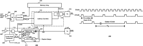
19. An integrated circuit comprising:
processing logic to generate a first signal; and
an interface circuit coupled to the processing logic, the interface circuit to send the first signal to a memory device, wherein, when decoded by a command decoder of the memory device, the first signal to cause a programmable timer of a clock gating circuit of the memory device to generate a clock signal having a predetermined frequency.