| CPC G02F 1/1533 (2013.01) [B23K 26/40 (2013.01); C03B 33/0222 (2013.01); C03B 33/04 (2013.01); C03B 33/074 (2013.01); E06B 3/66 (2013.01); G02F 1/155 (2013.01); G02F 1/161 (2013.01); G02F 2001/1555 (2013.01)] | 20 Claims |

|
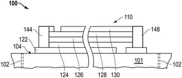
1. An electrochromic structure, comprising:
a substrate;
a first filament in the substrate extending in a direction substantially parallel to a thickness of the substrate;
an electrochromic stack on the substrate, wherein the electrochromic stack comprises:
a transparent conductive layer including a first portion and a second portion spaced apart from the first portion; and
an electrochromic layer disposed over the first portion and the second portion of the transparent conductive layer;
a first bus bar disposed on the first portion of the transparent conductive layer;
a second bus bar disposed on the second portion of the transparent conductive layer, wherein the substrate comprises an edge including a plurality of channels that are spaced apart from one another, wherein at least some of the plurality of channels extend through a thickness of the substrate.
|