| CPC G02F 1/13439 (2013.01) [G02F 1/133345 (2013.01); G02F 1/1323 (2013.01)] | 5 Claims |
|
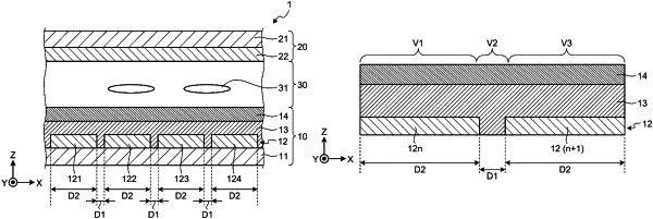
1. A liquid crystal panel comprising:
a first substrate that is a light-transmitting substrate;
a second substrate that is disposed facing the first substrate with a liquid crystal interposed between the first substrate and the second substrate and is a light-transmitting substrate;
a wiring layer provided on the first substrate on a side facing the liquid crystal and comprising a plurality of wiring lines arrayed in a predetermined direction;
an insulating layer stacked on the wiring layer on a side facing the liquid crystal;
a first electrode layer stacked on the insulating layer on a side facing the liquid crystal; and
a second electrode layer provided on the second substrate on a side facing the liquid crystal, wherein
a sheet resistance of the first electrode layer is higher than a sheet resistance of the wiring layer and a sheet resistance of the second electrode layer, and
the wiring layer and the first electrode layer are not electrically connected.
|