| CPC G02F 1/13338 (2013.01) [G02F 1/13306 (2013.01); G02F 1/133357 (2021.01); G02F 1/1339 (2013.01); G02F 1/134309 (2013.01); G02F 1/136286 (2013.01); G02F 1/1368 (2013.01)] | 18 Claims |

|
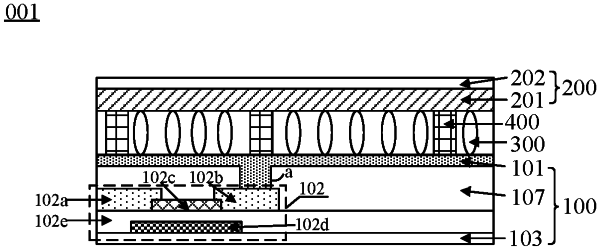
1. A liquid crystal handwriting board, comprising: a liquid crystal panel, and a drive assembly electrically connected to the liquid crystal panel;
wherein
the liquid crystal panel comprises: a first substrate and a second substrate that are opposite to each other, and a liquid crystal layer disposed between the first substrate and the second substrate, wherein the first substrate comprises a plurality of bulk pixel electrodes, and the second substrate comprises a planar common electrode; and
the drive assembly is configured to apply, based on position information of a region to be erased, a pixel voltage to a pixel electrode in the region to be erased in the case that the liquid crystal handwriting board is in an erasing mode, such that a voltage difference is developed between the pixel electrode in the region to be erased and the common electrode, wherein the first substrate further comprises a second planarization layer disposed on the pixel electrode;
wherein the first substrate further comprises: a plurality of thin-film transistors electrically connected to the drive assembly, wherein the pixel electrode is electrically connected to at least one of the plurality of thin-film transistors;
wherein the first substrate further comprises a first planarization layer disposed on the at least one thin-film transistor.
|