| CPC G02F 1/035 (2013.01) [G02F 1/225 (2013.01); G02F 1/212 (2021.01); G02F 2202/105 (2013.01)] | 17 Claims |

|
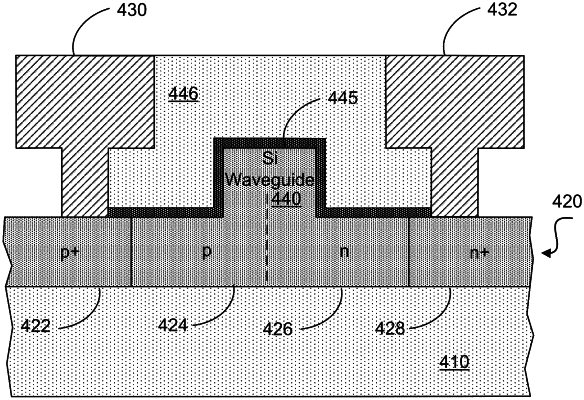
1. An optical switch structure comprising:
a first electrical contact;
a second electrical contact;
doped semiconductor regions forming a p-n junction, the doped semiconductor regions disposed between the first electrical contact and the second electrical contact; and
a waveguide structure disposed between the first electrical contact and the second electrical contact, the waveguide structure comprising:
a waveguide core including a core material characterized by a first index of refraction; and
a planar waveguide cladding coupled to the waveguide core, the first electrical contact, and the second electrical contact, wherein the planar waveguide cladding includes a cladding material characterized by a second index of refraction less than the first index of refraction and an isotope-enhanced Pockels effect.
|