| CPC G02B 30/36 (2020.01) [G02B 27/4255 (2013.01)] | 17 Claims |
|
1. A display device comprising:
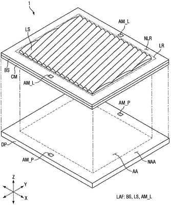
a display panel including an active region, an inactive region disposed adjacent to the active region, and a first alignment mark, wherein a plurality of sub-pixels is disposed in the active region, and the first alignment mark is positioned at a first distance in a first direction from an alignment reference pixel disposed adjacent to a boundary of the active region; and
an optical member including a plurality of lenses and a second alignment mark, wherein the plurality of lenses is disposed to be inclined at a first angle with respect to a direction in which the plurality of sub-pixels is arranged, and wherein the second alignment mark is positioned at the first distance in the first direction from the alignment reference pixel and is positioned at a second distance in a second direction, crossing the first direction, from the first alignment mark,
wherein the second alignment mark is misaligned with the first alignment mark,
wherein the second alignment mark is disposed on the plurality of lenses,
wherein the second alignment mark is disposed on a lens, among the plurality of lenses, overlapping the alignment reference pixel.
|