| CPC G01R 31/2889 (2013.01) [G01R 31/2863 (2013.01)] | 20 Claims |
|
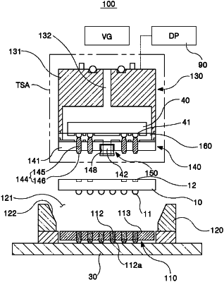
1. A test apparatus for a semiconductor package, comprising:
a lower test socket mounted on a tester providing a test signal, and connected to a lower terminal of a lower package to electrically connect the lower package to the tester;
a pusher configured to be able to be moved vertically by receiving a driving force from a driving unit;
an upper test socket mounted on the pusher, and having an electro-conductive part installed below the upper package to be electrically connected to a lower terminal of the upper package;
a vacuum picker mounted on a center of the upper test socket to be able to vacuum-adsorb the lower package; and
an inelastic insulating sheet installed between the upper test socket and the upper package, the inelastic insulating sheet having a through hole formed at a position thereof corresponding to the terminal of the upper package and the electro-conductive part, and having a vacuum space part formed in a lower surface thereof corresponding to the upper test socket.
|