| CPC F02D 41/28 (2013.01) [F02D 2041/288 (2013.01)] | 6 Claims |
|
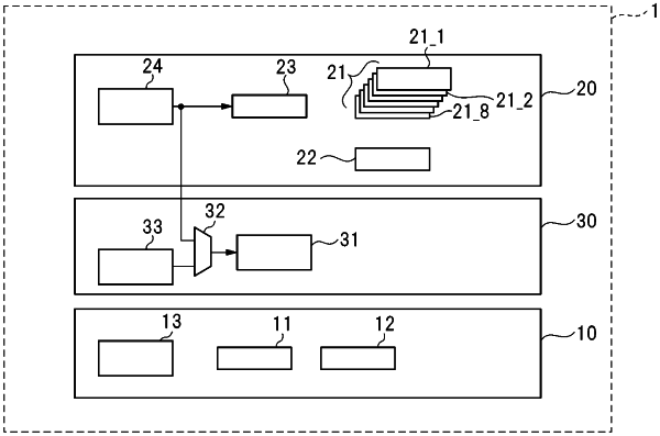
1. A semiconductor device comprising:
a frequency output circuit configured to output clock signals having a given frequency;
a circuit block configured to perform an operation in any one of a plurality of operation states; and
a standby controller coupled to the frequency output circuit and the circuit block, and configured to control the circuit block to transition to a standby mode,
wherein the standby controller comprises:
a control circuit configured to control the circuit block and output state information of the circuit block, and
a frequency selection circuit configured, in response to the state information, to output:
a frequency control signal to the frequency output circuit to control a frequency of the clock signals; and
a counting information signal to the control circuit to designate a timing of a state transition of the circuit block,
wherein the control circuit is further configured to control the circuit block to transition to the standby mode based on the counting information from the frequency selection circuit and the clock signals from the frequency output circuit.
|