| CPC H10N 70/8833 (2023.02) [H10B 61/10 (2023.02); H10N 70/043 (2023.02); H10N 70/063 (2023.02); H10N 70/841 (2023.02); H01L 29/36 (2013.01)] | 7 Claims |
|
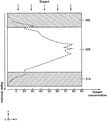
1. A method of manufacturing a memory device including a silicon oxide and a variable resistance element electrically coupled to the silicon oxide, comprising:
introducing a dopant into the silicon oxide from a first surface of the silicon oxide by ion implantation;
thinning the silicon oxide by etching the first surface of the silicon oxide with an ion beam; and
removing a first part of the thinned silicon oxide to leave a second part of the thinned silicon oxide, after the thinning of the silicon oxide.
|