| CPC H10N 70/841 (2023.02) [H10B 63/00 (2023.02); H10N 70/021 (2023.02)] | 20 Claims |
|
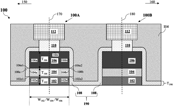
1. A memory device comprising:
a first electrode;
an insulating element arranged over the first electrode;
a second electrode arranged over the insulating element; wherein each of the first electrode, the insulating element, and the second electrode comprises a first side surface and a second side surface; wherein centers of the first electrode, the insulating element, and the second electrode are substantially vertically aligned; and wherein the first side surface and the second side surface of the second electrode are substantially vertically aligned with the first side surface and the second side surface of at least one of the insulating element and the first electrode;
a switching layer conformal to the first side surfaces and the second side surfaces of the second electrode and the insulating element; and
a conductive line electrically coupled to the second electrode,
wherein each of the first electrode, the insulating element, and the second electrode are cuboidal.
|