| CPC H10N 70/245 (2023.02) [H10N 70/011 (2023.02); H10N 70/24 (2023.02); H10N 70/826 (2023.02); H10N 70/828 (2023.02); H10N 70/8416 (2023.02)] | 20 Claims |
|
1. A semiconductor device, comprising:
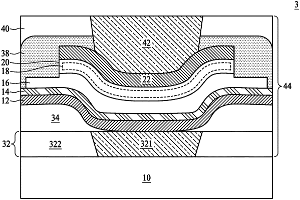
a bottom electrode;
a top electrode over the bottom electrode;
a switching layer between the bottom electrode and the top electrode, wherein the switching layer is configured to store data;
a capping layer in contact with the switching layer, wherein the capping layer is configured to extract active metal ions from the switching layer;
an ion reservoir region formed in the capping layer;
a diffusion barrier layer between the bottom electrode and the switching layer, wherein the diffusion barrier layer comprises palladium (Pd), cobalt (Co), or a combination thereof and is configured to obstruct diffusion of the active metal ions between the switching layer and the bottom electrode, and the diffusion barrier layer has a concaved top surface; and
a passivation layer covering a portion of the top electrode, and wherein the passivation layer directly contacts a top surface of the switching layer,
wherein an upper surface of the bottom electrode has a recess, and the bottom electrode includes an outer portion and an inner portion surrounded by the outer portion, and a lowermost surface of the outer portion is above a top surface of the inner portion.
|