| CPC H10N 60/815 (2023.02) [B82Y 10/00 (2013.01); G06F 30/392 (2020.01); G06N 10/00 (2019.01); H01L 24/16 (2013.01); H01L 24/17 (2013.01); H10N 69/00 (2023.02); H01L 2224/14179 (2013.01); H01L 2224/16148 (2013.01); H01L 2224/17179 (2013.01)] | 20 Claims |

|
1. A device comprising:
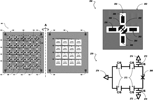
a plurality of quantum computing elements, wherein each quantum computing element of the plurality of quantum computing elements comprises at least three electrically conductive islands,
wherein the plurality of quantum computing elements together define an enclosed region, and
wherein, for each quantum computing element of the plurality of quantum computing elements, at least one electrically conductive island of the quantum computing element lacks a direct electrical connection to each other electrically conductive island of the quantum computing element.
|