| CPC H10N 50/80 (2023.02) [G11C 11/161 (2013.01); H01F 10/3254 (2013.01); H01F 10/3272 (2013.01); H10B 61/00 (2023.02); H10B 61/22 (2023.02); H10N 50/01 (2023.02); H10N 50/10 (2023.02); H10N 50/85 (2023.02)] | 20 Claims |
|
1. A magnetic tunnel junction device comprising:
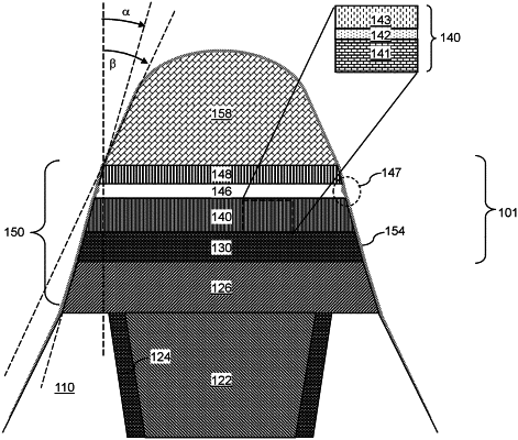
a pillar structure comprising, from bottom to top, a bottom electrode and a magnetic tunnel junction structure that contains a reference magnetization layer including a first ferromagnetic material, a tunnel barrier layer, and a free magnetization layer including a second ferromagnetic material;
a top electrode overlying the magnetic tunnel junction structure and comprising a metallic material containing a nonmagnetic metal element; and
a dielectric metal oxide layer extending from a sidewall of the pillar structure to a sidewall of the top electrode, wherein a lower portion of the dielectric metal oxide layer contacting the sidewall of the pillar structure comprises a composite dielectric metal oxide material containing a metal oxide of the first ferromagnetic material, a metal oxide of the second ferromagnetic material, and a metal oxide of the nonmagnetic metal element, wherein an average molar fraction of the metal oxide of the nonmagnetic metal element within the lower portion of the dielectric metal oxide layer is in a range from 0.001 to 0.5.
|