US 11,991,930 B2
Memory device and method for fabricating the same
Jung-Tang Wu, Kaohsiung (TW); Szu-Ping Tung, Taipei (TW); Szu-Hua Wu, Hsinchu County (TW); Shing-Chyang Pan, Hsinchu County (TW); and Meng-Yu Wu, Taichung (TW)
Assigned to TAIWAN SEMICONDUCTOR MANUFACTURING CO, LTD., Hsinchu (TW)
Filed by TAIWAN SEMICONDUCTOR MANUFACTURING CO, LTD., Hsinchu (TW)
Filed on Nov. 9, 2022, as Appl. No. 17/984,066.
Application 16/741,557 is a division of application No. 16/059,777, filed on Aug. 9, 2018, granted, now 10,535,816, issued on Jan. 14, 2020.
Application 17/984,066 is a continuation of application No. 17/112,861, filed on Dec. 4, 2020, granted, now 11,515,474.
Application 17/112,861 is a continuation of application No. 16/741,557, filed on Jan. 13, 2020, granted, now 10,862,026, issued on Dec. 8, 2020.
Claims priority of provisional application 62/590,182, filed on Nov. 22, 2017.
Prior Publication US 2023/0073308 A1, Mar. 9, 2023
This patent is subject to a terminal disclaimer.
Int. Cl. H01L 43/12 (2006.01); H01L 27/22 (2006.01); H01L 43/02 (2006.01); H10B 61/00 (2023.01); H10N 50/01 (2023.01); H10N 50/80 (2023.01)
CPC H10N 50/01 (2023.02) [H10B 61/22 (2023.02); H10N 50/80 (2023.02)] 20 Claims
OG exemplary drawing
 
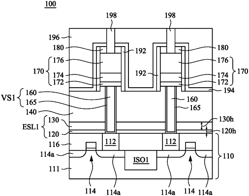
1. A structure, comprising:
a substrate;
a transistor on the substrate;
a contact on a source/drain region of the transistor;
an oxygen-free etch stop layer spanning the contact;
an oxygen-containing etch stop layer extending along a top surface of the oxygen-free etch stop layer;
a dielectric layer over the oxygen-containing etch stop layer;
a via passing through the dielectric layer, the oxygen-containing etch stop layer, and the oxygen-free etch stop layer and landing on the contact; and
a memory stack landing on the via.