| CPC H10K 77/111 (2023.02) [H01L 27/1218 (2013.01); H01L 27/124 (2013.01); H01L 29/78603 (2013.01); H01L 29/78633 (2013.01); H10K 50/80 (2023.02); H10K 59/131 (2023.02); H10K 59/1213 (2023.02); H10K 59/126 (2023.02); H10K 2102/311 (2023.02); Y02E 10/549 (2013.01)] | 15 Claims |
|
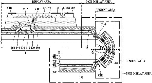
1. A display device comprising:
a flexible substrate including an active area and a non-display area, the non-display area including a bending area configured to be bent;
a link line including a first link line and a second link line in the non-display area;
a bending connection line including a first end connected to the first link line and a second end connected to the second link line, the bending connection line electrically connected with the first link line and the second link line on the flexible substrate;
a first buffer layer and a second buffer layer in the bending area of the flexible substrate; and
an inorganic layer that surrounds the bending connection line, the inorganic layer between the first buffer layer and the second buffer layer in the bending area of the flexible substrate,
wherein the first link line is connected to the first end of the bending connection line via a first contact hole, and the second link line is connected to the second end of the bending connection line via a second contact hole,
wherein the first buffer layer is directly under the inorganic layer and the second buffer layer is directly on the inorganic layer.
|