| CPC H10K 71/166 (2023.02) [C22C 38/08 (2013.01); C23C 14/042 (2013.01); C23C 14/24 (2013.01); H10K 71/00 (2023.02); H10K 71/164 (2023.02)] | 10 Claims |
|
1. A deposition mask including an iron (Fe) and a nickel (Ni) of metal materials for OLED pixel deposition, wherein the deposition mask comprises a metal plate including an iron (Fe)-nickel (Ni) alloy,
wherein the metal plate comprises a deposition region and a non-deposition region other than the deposition region for forming a deposition pattern, wherein the deposition region includes a plurality of effective portions and an ineffective portion other than the effective portions, wherein one of the effective portions includes:
a plurality of small surface holes formed on one surface of the deposition mask;
a plurality of large surface holes formed on another surface of the deposition mask opposite to the one surface;
a plurality of through-holes communicating the small surface holes and the large surface holes of the deposition mask; and
an island portion formed on the other surface of the deposition mask, and disposed between the plurality of through-holes,
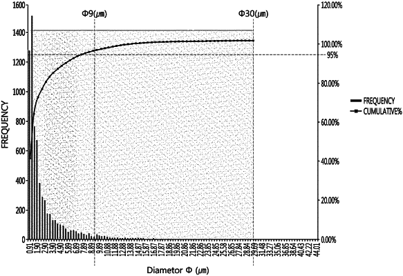
wherein the metal plate is formed of a plurality of crystal grains, and a maximum area of the crystal grains measured over an entire area of the metal plate is 700 μm2 or less, and wherein when measuring from small crystal grains in all crystal grains measured over the entire area of the metal plate, a maximum area of 95% of the small crystal grains is 60 μm2 or less.
|