US 11,991,913 B2
Semiconductor device including detection electrodes applicable for a touch sensor
Mitsuhide Miyamoto, Tokyo (JP); and Hajime Akimoto, Tokyo (JP)
Assigned to Japan Display Inc., Tokyo (JP)
Filed by Japan Display Inc., Tokyo (JP)
Filed on Jul. 12, 2022, as Appl. No. 17/862,926.
Application 17/862,926 is a continuation of application No. 17/173,610, filed on Feb. 11, 2021, granted, now 11,437,446.
Application 17/173,610 is a continuation of application No. 16/856,768, filed on Apr. 23, 2020, granted, now 10,957,748, issued on Mar. 23, 2021.
Application 16/856,768 is a continuation of application No. 16/453,493, filed on Jun. 26, 2019, granted, now 10,672,840, issued on Jun. 2, 2020.
Application 16/453,493 is a continuation of application No. 16/139,844, filed on Sep. 24, 2018, granted, now 10,381,421, issued on Aug. 13, 2019.
Application 16/139,844 is a continuation of application No. 15/833,557, filed on Dec. 6, 2017, granted, now 10,109,687, issued on Oct. 23, 2018.
Application 15/833,557 is a continuation of application No. 15/336,026, filed on Oct. 27, 2016, granted, now 9,871,083, issued on Jan. 16, 2018.
Claims priority of application No. 2016-006329 (JP), filed on Jan. 15, 2016.
Prior Publication US 2022/0344410 A1, Oct. 27, 2022
This patent is subject to a terminal disclaimer.
Int. Cl. H10K 59/40 (2023.01); G06F 3/041 (2006.01); G06F 3/044 (2006.01); H10K 50/11 (2023.01); H10K 50/17 (2023.01); H10K 50/842 (2023.01); H10K 50/844 (2023.01); H10K 59/122 (2023.01); H10K 59/35 (2023.01); H10K 77/10 (2023.01)
CPC H10K 59/40 (2023.02) [G06F 3/0412 (2013.01); G06F 3/04164 (2019.05); G06F 3/0446 (2019.05); H10K 50/11 (2023.02); H10K 50/17 (2023.02); H10K 50/171 (2023.02); H10K 50/8426 (2023.02); H10K 50/844 (2023.02); H10K 59/122 (2023.02); H10K 59/35 (2023.02); H10K 77/111 (2023.02); G06F 2203/04102 (2013.01); Y02E 10/549 (2013.01)] 17 Claims
OG exemplary drawing
 
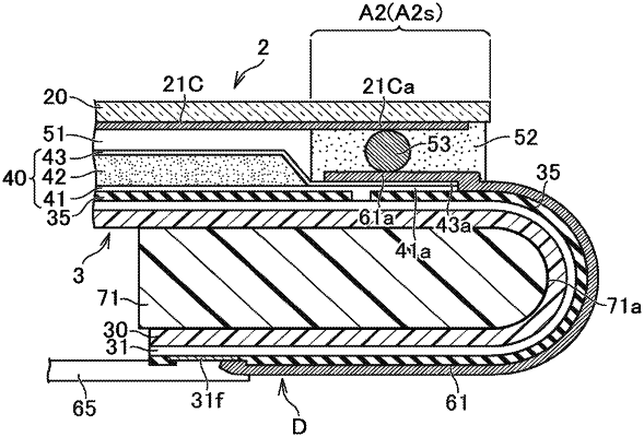
1. A semiconductor device comprising:
a substrate;
a first insulator on the substrate;
a second insulator on the first insulator;
a plurality of detection electrodes, the plurality of detection electrodes overlapping the second insulator in a planar view;
a terminal on the substrate, the terminal located along an edge of the substrate;
a first detection line electrically connected to the terminal; and
a second detection line electrically connected to one of the plurality of detection electrodes, wherein
the first detection line and the second detection line are electrically connected with each other at a contact portion,
the contact portion is located between the plurality of detection electrodes and an edge of the second insulator in the planar view,
the substrate is configured to be folded back at a bent portion,
the bent portion is between the contact portion and the terminal, and
the first detection line and the first insulator overlap at the bent portion in the planar view.