US 11,991,912 B2
Display panel and manufacturing method thereof
Wenliang Gong, Hubei (CN); and Wenxu Xianyu, Hubei (CN)
Assigned to WUHAN CHINA STAR OPTOELECTRONICS SEMICONDUCTOR DISPLAY TECHNOLOGY CO., LTD., Hubei (CN)
Appl. No. 17/053,186
Filed by WUHAN CHINA STAR OPTOELECTRONICS SEMICONDUCTOR DISPLAY TECHNOLOGY CO., LTD., Hubei (CN)
PCT Filed Jun. 24, 2020, PCT No. PCT/CN2020/098146
§ 371(c)(1), (2) Date Nov. 5, 2020,
PCT Pub. No. WO2021/243770, PCT Pub. Date Dec. 9, 2021.
Claims priority of application No. 202010490533.8 (CN), filed on Jun. 2, 2020.
Prior Publication US 2022/0285444 A1, Sep. 8, 2022
Int. Cl. H10K 59/38 (2023.01); C09D 7/63 (2018.01); C09D 101/28 (2006.01); C09D 133/26 (2006.01); C09D 139/02 (2006.01); C09D 147/00 (2006.01); H10K 50/84 (2023.01); H10K 50/86 (2023.01); H10K 71/00 (2023.01); C08K 5/098 (2006.01)
CPC H10K 59/38 (2023.02) [C09D 7/63 (2018.01); C09D 101/288 (2013.01); C09D 133/26 (2013.01); C09D 139/02 (2013.01); C09D 147/00 (2013.01); H10K 50/841 (2023.02); H10K 50/865 (2023.02); H10K 71/00 (2023.02); C08K 5/098 (2013.01)] 14 Claims
OG exemplary drawing
 
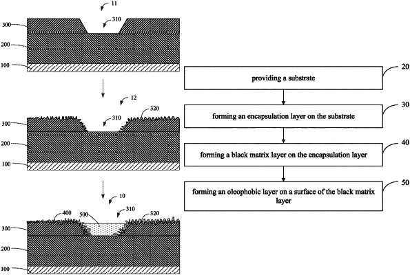
1. A display panel, comprising:
a substrate;
an encapsulation layer disposed on a surface of the substrate;
a black matrix layer disposed on the encapsulation layer, wherein the black matrix layer comprises a through hole, and the through hole extends through the black matrix layer to expose the encapsulation layer;
an oleophobic layer covering the black matrix layer;
wherein an upper surface of the black matrix layer comprises a microstructure, and a surface of the microstructure is provided with a polar anionic group.