| CPC H10K 59/131 (2023.02) [G02F 1/0107 (2013.01); G02F 1/133388 (2021.01); G02F 1/1339 (2013.01); G02F 1/136286 (2013.01); G02F 1/13629 (2021.01); G02F 1/161 (2013.01); G02F 1/1679 (2019.01); H10K 50/841 (2023.02)] | 15 Claims |
|
1. A display device comprising:
an array substrate including a pixel array disposed in a display area;
an encapsulation substrate; and
a sealing member disposed between the array substrate and the encapsulation substrate to combine the array substrate with the encapsulation substrate,
wherein the array substrate includes:
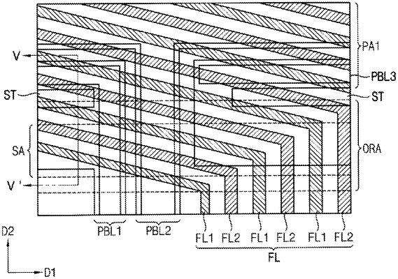
a signal transfer wiring overlapping the sealing member and electrically connected to the pixel array;
an insulation layer covering the signal transfer wiring and including an inorganic material;
a power transfer wiring disposed on the insulation layer, overlapping the sealing member and having a multi-wiring structure; and
an expansion pattern connected to the power transfer wiring, having a thickness smaller than a thickness of the power transfer wiring and overlapping the sealing member and the signal transfer wiring, wherein an outer edge of the expansion pattern is disposed within a sealing area where the sealing member is disposed,
wherein the power transfer wiring includes an upper conductive layer and a lower conductive layer, and the expansion pattern is disposed in a same layer as the upper conductive layer of the power transfer wiring,
wherein the expansion pattern or the upper conductive layer of the power transfer wiring fully covers an upper surface the lower conductive layer of the power transfer wiring in the sealing area.
|