| CPC H10K 59/131 (2023.02) [G09G 3/006 (2013.01)] | 16 Claims |
|
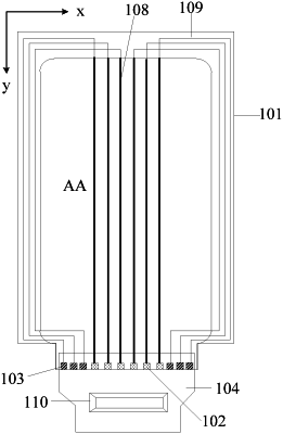
1. A display panel, comprising:
a display cell, comprising:
a plurality of display pins; and
a plurality of cell test pins;
wherein the display pins and the cell test pins are arranged in a bonding region of the display cell;
a chip on film, bonded to a side facing away from a display surface of the display cell, an orthographic projection of the chip on film on the display cell completely covering the display pins and the cell test pins;
a plurality of signal lines in a display region of the display cell; wherein the signal lines are electrically connected to the display pins in a one-to-one manner; and
a plurality of test lines arranged at a periphery of the display region of the display cell and electrically connected to the signal lines in a one-to-one manner; wherein the test lines are electrically connected to the cell test pins in a one-to-one manner.
|