| CPC H10K 59/131 (2023.02) [G09G 3/3275 (2013.01); G09G 2300/0876 (2013.01); H10K 59/1201 (2023.02)] | 20 Claims |
|
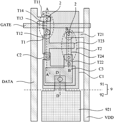
1. A display substrate, comprising a plurality of pixel regions, each of the pixel regions comprising a display region provided with a light emitting device and a driving region provided with a pixel circuit, the pixel circuit comprising at least one pixel transistor having a first electrode and a second electrode which are coupled to an active layer of the at least one pixel transistor through connection vias, respectively, wherein
the driving region is further provided with a first plate of a storage capacitor, the first plate is insulated from and overlapped with the first electrode and the second electrode of the at least one pixel transistor in a direction perpendicular to the display substrate, and the first plate is provided with openings at positions corresponding to at least some of the connection vias.
|