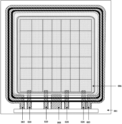
| CPC H10K 59/131 (2023.02) [H10K 50/844 (2023.02); H10K 59/121 (2023.02)] | 18 Claims |

|
1. A display substrate, comprising:
a base substrate;
a plurality of pixel units, wherein the plurality of pixel units are located on the base substrate;
at least one first power line; located on the base substrate;
a blocking structure, wherein the blocking structure surrounds the plurality of pixel units;
an auxiliary connection structure, comprising a first side surface and a second side surface which are opposite to each other, wherein the first side surface is closer to the plurality of pixel units than the second side surface;
a cathode layer, located on a side of the auxiliary connection structure away from the base substrate;
a first organic pattern, located on the side of the auxiliary connection structure away from the base substrate;
wherein the at least one first power line comprises a first portion and a second portion, the first portion is located on a side of the blocking structure away from the plurality of pixel units to receive a power signal, and the second portion is connected with the cathode layer by the auxiliary connection structure;
the second portion has a first connection position and a second connection position, the second portion is connected with the auxiliary connection structure at both the first connection position and the second connection position, and a distance between the first connection position and the blocking structure is larger than a distance between the second connection position and the blocking structure;
wherein a side surface of the first portion of the at least one first power line located on the side of the blocking structure away from the plurality of pixel units has a plurality of tooth-shaped convex structures, orthographic projections of the convex structures on the base substrate do not overlap with an orthographic projection of the blocking structure on the base substrate.
|