US 11,991,902 B2
Display device and method of manufacturing the same
Myung Hwan Kim, Yongin-si (KR); Suk Hoon Kang, Yongin-si (KR); Min Jae Kim, Yongin-si (KR); Hee Ra Kim, Yongin-si (KR); Beom Soo Shin, Yongin-si (KR); Hong Yeon Lee, Yongin-si (KR); and Baek Kyun Jeon, Yongin-si (KR)
Assigned to Samsung Display Co., Ltd., Yongin-si (KR)
Filed by SAMSUNG DISPLAY CO., LTD., Yongin-si (KR)
Filed on May 5, 2022, as Appl. No. 17/737,983.
Application 17/737,983 is a division of application No. 16/918,957, filed on Jul. 1, 2020, granted, now 11,335,747.
Application 16/918,957 is a division of application No. 15/867,882, filed on Jan. 11, 2018, granted, now 10,770,523, issued on Sep. 8, 2020.
Claims priority of application No. 10-2017-0086159 (KR), filed on Jul. 6, 2017.
Prior Publication US 2022/0262880 A1, Aug. 18, 2022
Int. Cl. H10K 59/122 (2023.01); H10K 50/11 (2023.01); H10K 50/813 (2023.01); H10K 50/822 (2023.01); H10K 59/12 (2023.01); H10K 59/173 (2023.01); H10K 71/00 (2023.01); H10K 71/13 (2023.01)
CPC H10K 59/122 (2023.02) [H10K 59/173 (2023.02); H10K 71/00 (2023.02); H10K 71/135 (2023.02); H10K 71/621 (2023.02); H10K 50/11 (2023.02); H10K 50/813 (2023.02); H10K 50/822 (2023.02); H10K 59/1201 (2023.02)] 6 Claims
OG exemplary drawing
 
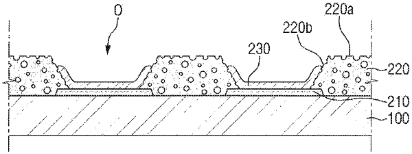
1. A method of manufacturing a display device, the method comprising:
forming an electrode on a base substrate;
forming a photoresist pattern on the base substrate, the photoresist pattern including a plurality of inorganic particles having inner holes and an opening exposing at least a portion of the electrode; and
forming a plurality of fine holes on a surface of the photoresist pattern by partially removing inorganic particles in the surface of the photoresist pattern, wherein partially removing the inorganic particles includes etching a surface of the photoresist pattern using a fluorinated gas to expose the inner holes in the inorganic particles.