| CPC H10K 50/854 (2023.02) [H10K 50/844 (2023.02); H10K 71/00 (2023.02); H10K 59/12 (2023.02); H10K 59/1201 (2023.02); H10K 59/17 (2023.02); H10K 2102/331 (2023.02)] | 8 Claims |
|
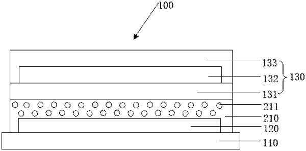
1. A display panel, comprising:
an array substrate;
an organic light emitting diode (OLED) light emitting device disposed on a side of the array substrate; and
a scattering layer dispoed on a side of the OLED light emitting device away from the array substrate, and covering the OLED light emitting device;
wherein the scattering layer has a plurality of micropores,
wherein diameters of the micropores range from 10 nm to 50 nm, and
wherein a material of the scattering layer is silicon nitride, and a thickness of the scattering layer ranges from 0.1 μm to 2 μm.
|