| CPC H10K 50/844 (2023.02) [H10K 50/115 (2023.02); H10K 50/865 (2023.02); H10K 59/38 (2023.02)] | 21 Claims |
|
1. A display apparatus comprising:
a substrate comprising a first area, and a second area adjacent to the first area;
a first light-emitting diode, a second light-emitting diode, and a third light-emitting diode that are arranged in the first area of the substrate and include a color emission layer;
an encapsulation layer overlapping the first light-emitting diode, the second light-emitting diode, and the third light-emitting diode, and comprising at least one inorganic layer and at least one organic layer;
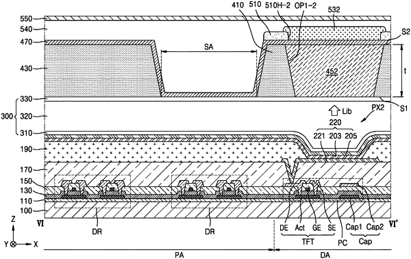
a first light shielding wall portion disposed on the encapsulation layer and not overlapping the first light-emitting diode, the second light-emitting diode, and the third light-emitting diode, the first light shielding wall portion comprising a 1-1-th opening portion, a 1-2-th opening portion, and a 1-3-th opening portion corresponding to the first light-emitting diode, the second light-emitting diode, and the third light-emitting diode, respectively; and
a second light shielding wall portion disposed on the encapsulation layer and overlapping the second area of the substrate; and
a driver arranged in the second area of the substrate and providing electrical signals to the first, second, and third light-emitting diodes, wherein
the first light shielding wall portion and the second light shielding wall portion are spaced apart from each other in a plan views,
at least a portion of the second light shielding wall portion overlaps the driver in a plan view.
|