US 11,991,891 B2
Display substrate and manufacturing method therefor, and display device
Zhuo Chen, Beijing (CN); and Siyi Yin, Beijing (CN)
Assigned to BEIJING BOE TECHNOLOGY DEVELOPMENT CO., LTD., Beijing (CN); and BOE TECHNOLOGY GROUP CO., LTD., Beijing (CN)
Appl. No. 17/266,673
Filed by BEIJING BOE TECHNOLOGY DEVELOPMENT CO., LTD., Beijing (CN); and BOE TECHNOLOGY GROUP CO., LTD., Beijing (CN)
PCT Filed Feb. 21, 2020, PCT No. PCT/CN2020/076173
§ 371(c)(1), (2) Date Feb. 8, 2021,
PCT Pub. No. WO2020/215868, PCT Pub. Date Oct. 29, 2020.
Claims priority of application No. 201910327425.6 (CN), filed on Apr. 23, 2019.
Prior Publication US 2021/0305527 A1, Sep. 30, 2021
Int. Cl. H01L 51/50 (2006.01); H10K 50/115 (2023.01); H10K 50/844 (2023.01); H10K 50/86 (2023.01); H10K 71/00 (2023.01)
CPC H10K 50/115 (2023.02) [H10K 50/844 (2023.02); H10K 50/865 (2023.02); H10K 71/00 (2023.02)] 18 Claims
OG exemplary drawing
 
1. A display substrate, comprising:
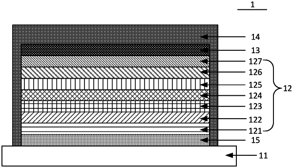
a base substrate, an electroluminescent device layer on the base substrate, and a light-absorbing layer on a light-emitting side of the electroluminescent device layer; wherein
the electroluminescent device layer is configured to emit initial light of a first color, wherein the initial light forms target light after passing through the light-absorbing layer, a full width at half maximum of an emission spectrum of the initial light is greater than a full width at half maximum of an emission spectrum of the target light, and the light-absorbing layer is on a side, distal from the base substrate, of the electroluminescent device layer.