| CPC H10B 63/84 (2023.02) [H01L 21/02565 (2013.01); H01L 21/8221 (2013.01); H01L 21/823475 (2013.01); H01L 27/0688 (2013.01); H01L 29/0673 (2013.01); H01L 29/24 (2013.01); H01L 29/42392 (2013.01); H01L 29/66969 (2013.01); H01L 29/78696 (2013.01); H01L 29/861 (2013.01); H10B 43/20 (2023.02); H10B 63/20 (2023.02); H10B 63/30 (2023.02); H10N 70/011 (2023.02); H10B 43/35 (2023.02); H10N 70/20 (2023.02)] | 20 Claims |
|
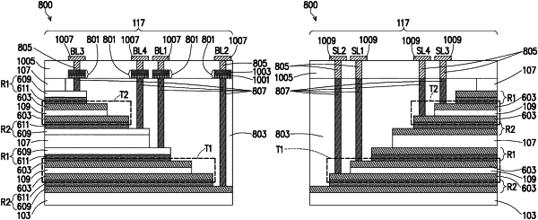
1. A method of forming a memory device, the method comprising:
forming a multilayer stack, the multilayer stack comprising:
a first conductive layer;
a first resistive layer over the first conductive layer;
a second conductive layer over the first resistive layer;
a first channel layer over the second conductive layer;
a third conductive layer over the first channel layer;
a second resistive layer over the third conductive layer; and
a fourth conductive layer over the second resistive layer;
forming a first dielectric layer over the multilayer stack;
forming a first conductive via through the first dielectric layer to the second conductive layer;
forming a second conductive via through the first dielectric layer to the third conductive layer;
forming a third conductive via through the first dielectric layer to the first conductive layer;
forming a fourth conductive via through the first dielectric layer to the fourth conductive layer;
forming a first diode on the first dielectric layer, the first diode being coupled to the third conductive via; and
forming a second diode on the first dielectric layer, the second diode being coupled to the fourth conductive via.
|